CLC109
Description
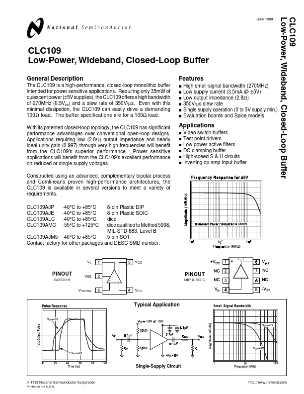
The CLC109 is a high-performance, closed-loop monolithic buffer intended for power sensitive applications. Requiring only 35mW of quiescent power (±5V supplies), the CLC109 offers a high bandwidth of 270MHz (0.5Vpp) and a slew rate of 350V/µs.